Hello everyone! Today, I am excited to share a project that marks a significant milestone in my PCB design journey. While my previous work mostly featured 2-layer boards, it was time to step into the “major leagues” and tackle professional industry standards.
This board was designed as part of an advanced course hosted by Robert Feranec (founder of Fedevel Academy). Robert is a world-class expert, and his courses are renowned for their rigorous focus on the high-quality engineering standards used by top-tier tech companies.
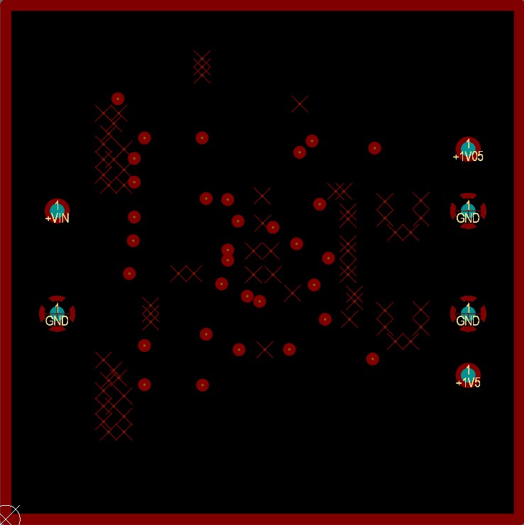
Technical Specifications & Stackup
This is my first fully functional 6-layer board. Moving from two layers to six is more than just having extra space for traces; it requires a completely different mindset regarding signal integrity and power distribution.
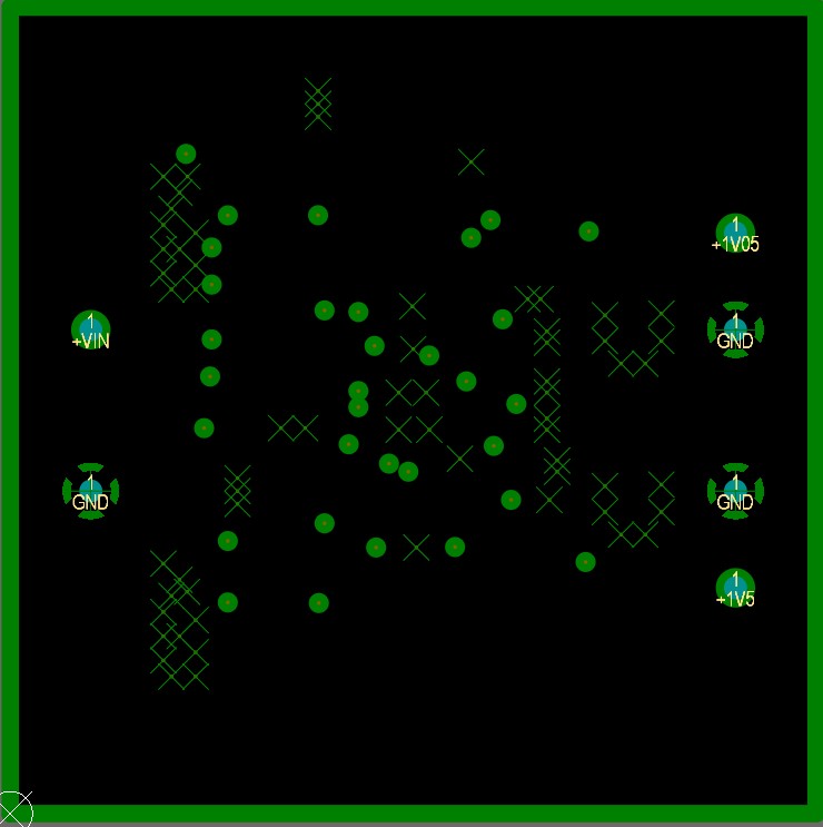
The Layer Stackup I implemented:
- L1 (Top): Primary power rails.
- L2 (GND): Full ground plane – critical for shielding and providing a clean current return path.
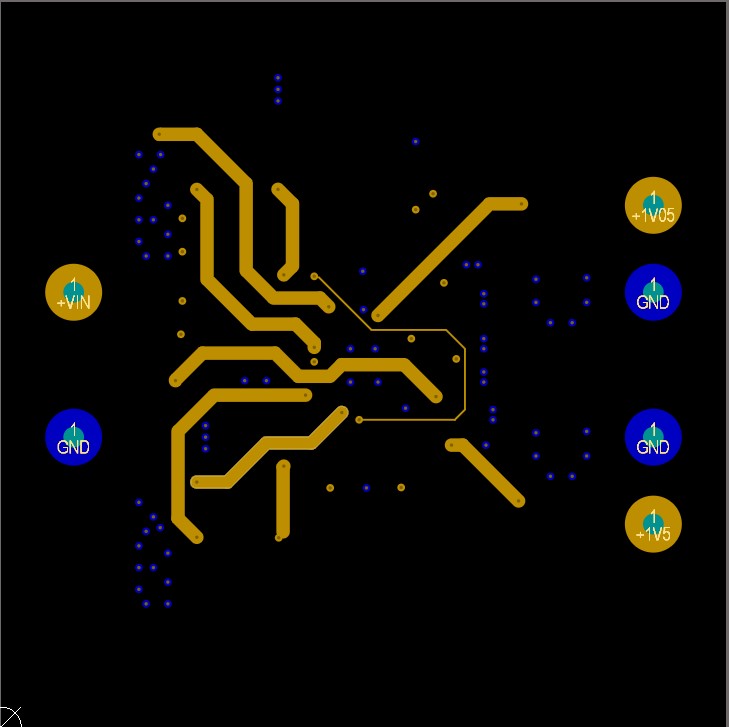
- L3 / L4: High-speed signals and, Internal signal layers.
- L5 (GND): Secondary reference plane to ensure system stability.
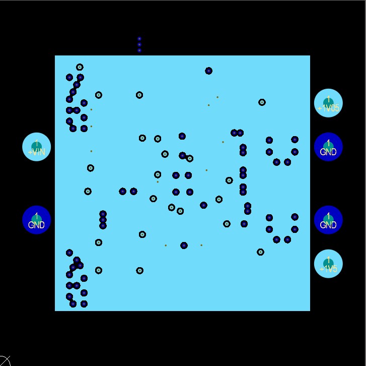
- L6 (Bottom): Bottom signal layer.
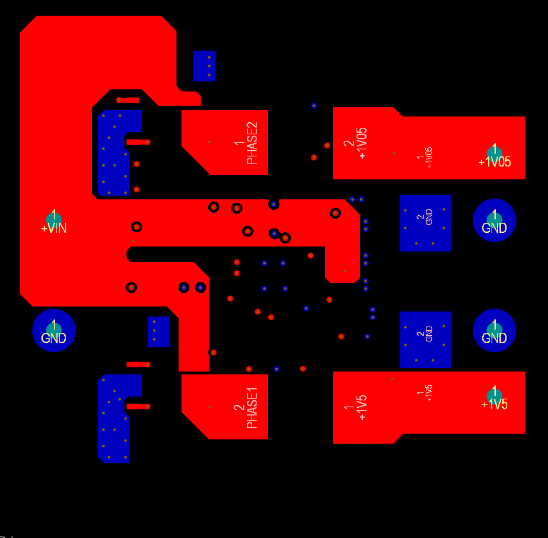
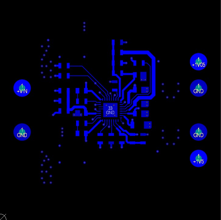
The Heart of the System: ISL6236A
The centerpiece of this design is the ISL6236A, an advanced power controller. The design process required high precision in component configuration:
- All configuration resistors were carefully selected to allow the chip to operate in its full configuration.
- In the current setup, the circuit generates two stable output voltages: 1.5V and 1.05V.
- A key challenge was the layout of the high-current section, ensuring minimal current loops and efficient heat dissipation.
What I’ve Learned
I completed this project step-by-step following Robert Feranec’s proven methodology. While the design process was based on the course guidelines, manually routing the entire 6-layer layout allowed me to truly “feel” the principles that are impossible to fully grasp on simple 2-layer boards.
Through this project, I gained practical experience in:
- Ground Plane Management: Understanding how critical a continuous return path is to avoid interference and EMI issues.
- Power Distribution Network (PDN) Optimization: How to properly route wide power traces and strategically place decoupling capacitors.
- High-Density Design: Fitting complex logic into a tight space while maintaining professional standards and serviceability.
I am incredibly satisfied with the final result. Although I relied on the extensive expertise provided by Fedevel Academy, I feel that these professional design standards are now a permanent part of my engineering toolkit. This is just the beginning—I am already planning future projects to apply these skills even further!
Fun Fact: This project feels like a full-circle moment for me. During my very first internship, when I officially started my PCB adventure, I was working on a Buck converter as well—but back then, it was a simple 2-layer board. Seeing how far I’ve come from those first steps to this advanced 6-layer design is a huge personal win!
See you on my next projects 🙂